|
Electronic Components Datasheet Search |
|
|
Electronic Components Datasheet Search |
|
AD823ARZ-R7 Datasheet(PDF) 14 Page - Analog Devices |
|
|
|||||||||||||||||||||||||||||
AD823ARZ-R7 Datasheet(HTML) 14 Page - Analog Devices |
|
|
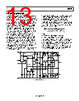
14 / 20 page  AD823 Data Sheet Rev. E | Page 14 of 20 OUTPUT IMPEDANCE The low frequency open-loop output impedance of the common- emitter output stage used in this design is approximately 30 kΩ. Although this is significantly higher than a typical emitter follower output stage, when it is connected with feedback, the output impedance is reduced by the open-loop gain of the op amp. With 109 dB of open-loop gain, the output impedance is reduced to <0.2 Ω. At higher frequencies, the output impedance rises as the open-loop gain of the op amp drops; however, the output also becomes capacitive due to the integrator capacitors C1 and C2. This prevents the output impedance from ever becoming excessively high (see Figure 18), which can cause stability problems when driving capacitive loads. In fact, the AD823 has excellent cap-load drive capability for a high frequency op amp. Figure 34 shows the AD823 connected as a follower while driving 470 pF direct capacitive load. Under these conditions, the phase margin is approximately 20°. If greater phase margin is desired, a small resistor can be used in series with the output to decouple the effect of the load capacitance from the op amp (see Figure 26). In addition, running the part at higher gains also improves the capacitive load drive capability of the op amp. VOUT S1N C1 S1P C5 R1 R1 gmVI gmVI gm2 C2 R2 Figure 37. Small Signal Schematic |
|
|
Link URL |
| Does ALLDATASHEET help your business so far? [ DONATE ] |
About Alldatasheet | Advertisement | Contact us | Privacy Policy | Link to Datasheet | Link Exchange | Manufacturer List All Rights Reserved©Alldatasheet.com |
| Russian : Alldatasheetru.com | Korean : Alldatasheet.co.kr | Spanish : Alldatasheet.es | French : Alldatasheet.fr | Italian : Alldatasheetit.com Portuguese : Alldatasheetpt.com | Polish : Alldatasheet.pl | Vietnamese : Alldatasheet.vn Indian : Alldatasheet.in | Mexican : Alldatasheet.com.mx | British : Alldatasheet.co.uk | New Zealand : Alldatasheet.co.nz |
|
Family Site : ic2ic.com |
icmetro.com |
 English ▼
 English
 Chinese
 German
 Japanese
 Russian
 Korean
 Spanish
 French
 Italian
 Portuguese
 Polish
 Vietnamese
 Indian
 Mexican
 British
 New Zealand