|
Electronic Components Datasheet Search |
|
|
Electronic Components Datasheet Search |
|
RC19302A00AGNT#BD0 Datasheet(PDF) 1 Page - Renesas Technology Corp |
|
|
|||||||||||||||||||||||||||||
RC19302A00AGNT#BD0 Datasheet(HTML) 1 Page - Renesas Technology Corp |
|
|
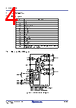
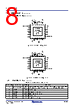
1 / 58 page  Datasheet R31DS0210EU0106 Rev.1.06 Page 1 May 11, 2026 © 2025-2026 Renesas Electronics Description The RC193xx (RC19302, RC19304, RC19308) ultra- high performance clock muxes support PCIe Gen 1-7. They provide a Loss-Of-Signal (LOS) output for system monitoring and redundancy. The devices also incorporate Power Down Tolerance (PDT), Flexible Power Sequencing (FPS), and Automatic Clock Parking (ACP) features, easing system design. They can drive both source-terminated and double- terminated loads, operating up to 400MHz. The family offers 2, 4, or 8 Low-Power (LP) HCSL output pairs in 3 × 3, 4 × 4, and 6 × 6 mm packages. The buffers support both Common Clock (CC) and Independent Reference (IR) PCIe clock architectures. Applications ▪ Cloud/High-performance computing ▪ nVME storage ▪ Networking ▪ AI Accelerators Features ▪ Very Low Additive Phase Jitter: • PCIe Gen5 CC: 6.9fs RMS (typ.) • PCIe Gen6 CC: 4.1fs RMS (typ.) • PCIe Gen7 CC: 2.9fs RMS (typ.) • DB2000Q: 11.5fs RMS (typ.) • 12kHz - 20MHz (156.25MHz): 42.8fs RMS (typ.) ▪ 2:N or dual x 1:N/2 modes (N is number of outputs) ▪ Power Down Tolerant (PDT) inputs ▪ Flexible Startup Sequencing (FSS) ▪ Automatic Clock Parking (ACP) upon loss of selected CLKIN ▪ Spread-spectrum tolerant ▪ CLKIN accepts HCSL or LVDS signal levels ▪ Dedicated OEb pin per output ▪ -40 to +105°C, 1.8V ± 5% operation ▪ Devices provide: • Pin or SMBus selectable 34Ω, 85Ω, or 100Ω differential output impedance • Pin or SMBus selectable output slew rate • Pin or SMBus selectable output amplitude • 9 SMBus addresses plus write protection Figure 1. Simplified Block Diagram and Mux Logic CLKSEL_tri 0 1 M Bank 0 CLKIN0 CLKIN1 CLKIN0 Bank 1 CLKIN0 CLKIN1 CLKIN1 CLKb3 CLK3 CLK0 CLKb0 Clock Detect LOSb 1 M 0 1 M 0 CLKSEL_tri CLKb7 CLK7 CLK4 CLKb4 Bank 0 CLKIN1 CLKINb 1 CLKIN0 CLKINb 0 Ban k 1 OEb[7:0] 2, 4 , or 8 Outputs 8 2, 4 , or 8 O utput Enables RC193xx PCIe Gen7 1.8V 2-Input Clock Mux Family with LOS |
Similar Part No. - RC19302A00AGNT#BD0 |
|
Similar Description - RC19302A00AGNT#BD0 |
|
|
Link URL |
| Does ALLDATASHEET help your business so far? [ DONATE ] |
About Alldatasheet | Advertisement | Contact us | Privacy Policy | Link to Datasheet | Link Exchange | Manufacturer List All Rights Reserved©Alldatasheet.com |
| Russian : Alldatasheetru.com | Korean : Alldatasheet.co.kr | Spanish : Alldatasheet.es | French : Alldatasheet.fr | Italian : Alldatasheetit.com Portuguese : Alldatasheetpt.com | Polish : Alldatasheet.pl | Vietnamese : Alldatasheet.vn Indian : Alldatasheet.in | Mexican : Alldatasheet.com.mx | British : Alldatasheet.co.uk | New Zealand : Alldatasheet.co.nz |
|
Family Site : ic2ic.com |
icmetro.com |
 English ▼
 English
 Chinese
 German
 Japanese
 Russian
 Korean
 Spanish
 French
 Italian
 Portuguese
 Polish
 Vietnamese
 Indian
 Mexican
 British
 New Zealand