|
Electronic Components Datasheet Search |
|
|
Electronic Components Datasheet Search |
|
IDT74FCT373C Datasheet(PDF) 3 Page - Integrated Device Technology |
|
|
|||||||||||||||||||||||||||||
IDT74FCT373C Datasheet(HTML) 3 Page - Integrated Device Technology |
|
|
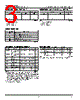
3 / 8 page  7.12 3 IDT54/74FCT373/533/573/A/C FAST CMOS OCTAL TRANSPARENT LATCHES MILITARY AND COMMERCIAL TEMPERATURE RANGES FUNCTION TABLE (FCT533) (1) FUNCTION TABLE (FCT373 and FCT573) (1) PIN DESCRIPTION 2602 tbl 07 ABSOLUTE MAXIMUM RATINGS (1) CAPACITANCE (TA = +25 °C, f = 1.0MHz) Symbol Parameter Conditions Typ. Max. Unit CIN Input Capacitance VIN = 0V 6 10 pF COUT Output Capacitance VOUT = 0V 8 12 pF NOTE: 2602 tbl 02 1. This parameter is measured at characterization but not tested. NOTE: 2602 tbl 05 1. H = HIGH Voltage Level L = LOW Voltage Level X = Don’t Care Z = High Impedance NOTE: 2602 tbl 06 1. H = HIGH Voltage Level L = LOW Voltage Level X = Don’t Care Z = High Impedance NOTES: 2602 tbl 01 1. Stresses greater than those listed under ABSOLUTE MAXIMUM RATINGS may cause permanent damage to the device. This is a stress rating only and functional operation of the device at these or any other conditions above those indicated in the operational sections of this specification is not implied. Exposure to absolute maximum rating conditions for extended periods may affect reliability. No terminal voltage may exceed VCC by +0.5V unless otherwise noted. 2. Input and VCC terminals only. 3. Outputs and I/O terminals only. Symbol Rating Commercial Military Unit VTERM(2) Terminal Voltage with Respect to GND –0.5 to +7.0 –0.5 to +7.0 V VTERM(3) Terminal Voltage with Respect to GND –0.5 to VCC –0.5 to VCC V TA Operating Temperature 0 to +70 –55 to +125 °C TBIAS Temperature Under Bias –55 to +125 –65 to +135 °C TSTG Storage Temperature –55 to +125 –65 to +150 °C PT Power Dissipation 0.5 0.5 W IOUT DC Output Current 120 120 mA Inputs Outputs DN LE OE OE ON HH L H LH L L XXH Z Inputs Outputs DN LE OE OE O ON HH L L LH L H XXH Z Pin Names Description DN Data Inputs LE Latch Enable Input (Active HIGH) OE Output Enable Input (Active LOW) ON 3-State Outputs ON Complementary 3-State Outputs |
|
|
Link URL |
| Does ALLDATASHEET help your business so far? [ DONATE ] |
About Alldatasheet | Advertisement | Contact us | Privacy Policy | Link to Datasheet | Link Exchange | Manufacturer List All Rights Reserved©Alldatasheet.com |
| Russian : Alldatasheetru.com | Korean : Alldatasheet.co.kr | Spanish : Alldatasheet.es | French : Alldatasheet.fr | Italian : Alldatasheetit.com Portuguese : Alldatasheetpt.com | Polish : Alldatasheet.pl | Vietnamese : Alldatasheet.vn Indian : Alldatasheet.in | Mexican : Alldatasheet.com.mx | British : Alldatasheet.co.uk | New Zealand : Alldatasheet.co.nz |
|
Family Site : ic2ic.com |
icmetro.com |
 English ▼
 English
 Chinese
 German
 Japanese
 Russian
 Korean
 Spanish
 French
 Italian
 Portuguese
 Polish
 Vietnamese
 Indian
 Mexican
 British
 New Zealand