|
Electronic Components Datasheet Search |
|
|
Electronic Components Datasheet Search |
|
AD8251ARMZ-R7 Datasheet(PDF) 21 Page - Analog Devices |
|
|
|||||||||||||||||||||||||||||
AD8251ARMZ-R7 Datasheet(HTML) 21 Page - Analog Devices |
|
|
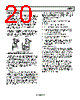
21 / 25 page  AD8251 Rev. B | Page 20 of 24 RF INTERFERENCE DRIVING AN ADC RF rectification is often a problem when amplifiers are used in applications where there are strong RF signals. The disturbance can appear as a small dc offset voltage. High frequency signals can be filtered with a low-pass RC network placed at the input of the instrumentation amplifier, as shown in Figure 58. The filter limits the input signal bandwidth according to the following relationship: An instrumentation amplifier is often used in front of an ADC to provide CMRR. Usually, instrumentation amplifiers require a buffer to drive an ADC. However, the low output noise, low distortion, and low settle time of the AD8251 make it an excellent ADC driver. In Figure 59, a 1 nF capacitor and a 49.9 Ω resistor create an antialiasing filter for the AD7612. The 1 nF capacitor stores and delivers the necessary charge to the switched capacitor input of the ADC. The 49.9 Ω series resistor reduces the burden of the 1 nF load from the amplifier and isolates it from the kickback current injected from the switched capacitor input of the AD7612. Selecting too small a resistor improves the correlation between the voltage at the output of the AD8251 and the voltage at the input of the AD7612 but may destabilize the AD8251. A trade- off must be made between selecting a resistor small enough to maintain accuracy and large enough to maintain stability. ) C C ( R 1 FilterFreq C D DIFF + = 2 π 2 C CM RC 1 FilterFreq π 2 = where CD ≥ 10 CC. R R AD8251 +15V +IN –IN 0.1µF 10µF 10µF 0.1µF REF VOUT –15V CD CC CC 0.1 μF 0.1 μF 1nF 49.9 Ω AD7612 ADR435 +12V –12V +5V +15V –15V A0 A1 WR +IN –IN 10 μF0.1µF 10 μF0.1µF REF AD8251 DGND DGND Figure 58. RFI Suppression Values of R and CC should be chosen to minimize RFI. A mismatch between the R × CC at the positive input and the R × CC at negative input degrades the CMRR of the AD8251. By using a value of CD that is 10 times larger than the value of C Figure 59. Driving an ADC C , the effect of the mismatch is reduced and performance is improved. |
|
|
Link URL |
| Does ALLDATASHEET help your business so far? [ DONATE ] |
About Alldatasheet | Advertisement | Contact us | Privacy Policy | Link to Datasheet | Link Exchange | Manufacturer List All Rights Reserved©Alldatasheet.com |
| Russian : Alldatasheetru.com | Korean : Alldatasheet.co.kr | Spanish : Alldatasheet.es | French : Alldatasheet.fr | Italian : Alldatasheetit.com Portuguese : Alldatasheetpt.com | Polish : Alldatasheet.pl | Vietnamese : Alldatasheet.vn Indian : Alldatasheet.in | Mexican : Alldatasheet.com.mx | British : Alldatasheet.co.uk | New Zealand : Alldatasheet.co.nz |
|
Family Site : ic2ic.com |
icmetro.com |
 English ▼
 English
 Chinese
 German
 Japanese
 Russian
 Korean
 Spanish
 French
 Italian
 Portuguese
 Polish
 Vietnamese
 Indian
 Mexican
 British
 New Zealand