|
Electronic Components Datasheet Search |
|
|
Electronic Components Datasheet Search |
|
MIPSZ2012D2R2 Datasheet(PDF) 25 Page - STMicroelectronics |
|
|
|||||||||||||||||||||||||||||
MIPSZ2012D2R2 Datasheet(HTML) 25 Page - STMicroelectronics |
|
|
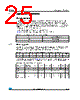
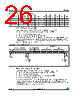
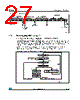
25 / 48 page  TS4621B Application information Doc ID 022194 Rev 2 25/48 4 Application information 4.1 I2C bus interface In compliance with the I²C protocol, the TS4621B uses a serial bus to control the chip’s functions with the clock (SCL) and data (SDA) wires. These two lines are bi-directional (open collector) and require an external pull-up resistor (typically 10 k Ω). The maximum clock frequency in fast mode specified by the I²C standard is 400 kHz, which the TS4621B supports. In this application, the TS4621B is always the slave device and the controlling microcontroller MCU is the master device. The slave address of the TS4621B is 1100 000x (C0h). Table 8 summarizes the pin descriptions for the I²C bus interface. 4.1.1 I²C bus operation The host MCU can write to the TS4621B control register to control the TS4621B, and read from the control register to obtain a configuration from the TS4621B. The TS4621B is addressed by the byte consisting of the 7-bit slave address and the R/W bit. There are four control registers (Table 10) named CR1 to CR4. In read mode, all the control registers can be accessed. In write mode, only CR1, CR2 and CR3 can be addressed. Table 8. Pin description of the I²C bus interface Pin Functional description SDA Serial data pin SCL Clock input pin Table 9. First byte after the START message for addressing the device A6 A5 A4 A3 A2 A1 A0 R/W 11 000 00 X Table 10. Summary of control registers Description Register address D7 D6 D5 D4 D3 D2 D1 D0 CR1 1 HP_EN_L HP_EN_R 0 0 SC_L SC_R T_SH SWS CR2 volume control 2 Mute_L Mute_R Volume control 0 CR3 3 0 0 0 0 0 0 HiZ_L HiZ_R CR4 identification 4 01 0 0 0 0 0 0 |
|
Link URL |
| Does ALLDATASHEET help your business so far? [ DONATE ] |
About Alldatasheet | Advertisement | Contact us | Privacy Policy | Link to Datasheet | Link Exchange | Manufacturer List All Rights Reserved©Alldatasheet.com |
| Russian : Alldatasheetru.com | Korean : Alldatasheet.co.kr | Spanish : Alldatasheet.es | French : Alldatasheet.fr | Italian : Alldatasheetit.com Portuguese : Alldatasheetpt.com | Polish : Alldatasheet.pl | Vietnamese : Alldatasheet.vn Indian : Alldatasheet.in | Mexican : Alldatasheet.com.mx | British : Alldatasheet.co.uk | New Zealand : Alldatasheet.co.nz |
|
Family Site : ic2ic.com |
icmetro.com |
 English ▼
 English
 Chinese
 German
 Japanese
 Russian
 Korean
 Spanish
 French
 Italian
 Portuguese
 Polish
 Vietnamese
 Indian
 Mexican
 British
 New Zealand