|
Electronic Components Datasheet Search |
|
|
Electronic Components Datasheet Search |
|
LTC1480IS8 Datasheet(PDF) 4 Page - Linear Technology |
|
|
|||||||||||||||||||||||||||||
LTC1480IS8 Datasheet(HTML) 4 Page - Linear Technology |
|
|
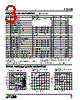
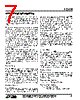
4 / 8 page  4 LTC1480 TYPICAL PERFORMANCE CHARACTERISTICS PIN FUNCTIONS high, the driver outputs will be fed back to the receiver and the receive output will correspond to the driver input. DI (Pin 4): Driver Input. If the driver outputs are enabled (DE HIGH) then a low on DI forces the outputs A LOW and B HIGH. A HIGH on DI with the driver outputs enabled will force A HIGH and B LOW. GND (Pin 5): Ground. A (Pin 6): Driver Output/Receiver Input. B (Pin 7): Driver Output/Receiver Input. VCC (Pin 8): Positive Supply. 3.0V < VCC < 3.6V. RO (Pin 1): Receiver Output. If the receiver output is enabled (RE LOW) and A > B by 200mV, then RO will be HIGH. If A < B by 200mV, then RO will be LOW. RE (Pin 2): Receiver Output Enable. A LOW enables the receiver output, RO. A HIGH input forces the receiver output into a high impedance state. DE (Pin 3): Driver Outputs Enable. A HIGH on DE enables the driver output. A, B and the chip will function as a line driver. A low input will force the driver outputs into a high impedance state and the chip will function as a line receiver. If RE is high and DE is LOW, the part will enter a low power (1 µA) shutdown state. If RE is low and DE is Receiver Output Low Voltage vs Output Current Receiver Output High Voltage vs Output Current OUTPUT VOLTAGE (V) 3.30 –8 –10 –12 1.30 LT1480 • TPC06 –6 –4 0 2.80 2.30 1.80 –2 –16 –14 3.05 2.55 2.05 1.55 VCC = 3.3V TA = 25°C OUTPUT VOLTAGE (V) 0 15 20 25 1.6 LTC1480 • TPC05 10 5 0 0.2 0.4 0.6 1.0 1.4 1.8 0.8 1.2 2.0 VCC = 3.3V TA = 25°C Driver Skew vs Temperature TEMPERATURE ( °C) –40 6.5 20 LT1480 • TPC04 5.0 4.0 –20 0 40 3.5 3.0 7.0 6.0 5.5 4.5 60 80 100 VCC = 3.3V Receiver tPLH – tPHL vs Temperature TEMPERATURE ( °C) –40 12 10 8 6 4 2 0 20 60 LT1480 • TPC07 –20 0 40 80 100 VCC = 3.3V Receiver Output Low Voltage vs Temperature TEMPERATURE ( °C) –40 0.4 0.5 0.6 20 60 LTC1480 • TPC08 0.3 0.2 –20 0 40 80 100 0.1 0 VCC = 3.3V 1 = 8mA Receiver Output High Voltage vs Temperature TEMPERATURE ( °C) –40 2.0 2.4 3.0 0 40 60 LTC1480 • TPC09 2.2 2.8 2.6 –20 20 80 100 VCC = 3.3V 1 = 8mA |
|
|
Link URL |
| Does ALLDATASHEET help your business so far? [ DONATE ] |
About Alldatasheet | Advertisement | Contact us | Privacy Policy | Link to Datasheet | Link Exchange | Manufacturer List All Rights Reserved©Alldatasheet.com |
| Russian : Alldatasheetru.com | Korean : Alldatasheet.co.kr | Spanish : Alldatasheet.es | French : Alldatasheet.fr | Italian : Alldatasheetit.com Portuguese : Alldatasheetpt.com | Polish : Alldatasheet.pl | Vietnamese : Alldatasheet.vn Indian : Alldatasheet.in | Mexican : Alldatasheet.com.mx | British : Alldatasheet.co.uk | New Zealand : Alldatasheet.co.nz |
|
Family Site : ic2ic.com |
icmetro.com |
 English ▼
 English
 Chinese
 German
 Japanese
 Russian
 Korean
 Spanish
 French
 Italian
 Portuguese
 Polish
 Vietnamese
 Indian
 Mexican
 British
 New Zealand