|
Electronic Components Datasheet Search |
|
|
Electronic Components Datasheet Search |
|
LTC1480IS8 Datasheet(PDF) 6 Page - Linear Technology |
|
|
|||||||||||||||||||||||||||||
LTC1480IS8 Datasheet(HTML) 6 Page - Linear Technology |
|
|
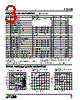
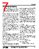
6 / 8 page  6 LTC1480 SWITCHI G TI E WAVEFOR S Figure 6. Driver Enable and Disable Times 1.5V 2.3V 2.3V tZH(SHDN), tZH tZL(SHDN), tZL 1.5V tLZ 0.5V 0.5V tHZ OUTPUT NORMALLY LOW OUTPUT NORMALLY HIGH 3V 0V DE 3.3V VOL VOH 0V A, B A, B LTC1480 • F06 f = 1MHz, tr ≤ 10ns, tf ≤ 10ns Figure 7. Receiver Propagation Delays 1.5V tPHL RO –VOD2 A – B 0V 0V 1.5V tPLH OUTPUT INPUT VOD2 VOL VOH LTC1480 • F07 f = 1MHz, tr ≤ 10ns, tf ≤ 10ns Figure 8. Receiver Enable and Disable Times 1.5V tZL(SHDN), tZL tZH(SHDN), tZH 1.5V 1.5V 1.5V tLZ 0.5V 0.5V tHZ OUTPUT NORMALLY LOW OUTPUT NORMALLY HIGH 3V 0V RE 3.3V VOL VOH 0V RO RO LTC1480 • F08 f = 1MHz, tr ≤ 10ns, tf ≤ 10ns APPLICATIO S I FOR ATIO CMOS Output Driver The LTC1480 transceiver provides full RS485 compatibil- ity while operating from a single 3.3V supply. The RS485 specification requires that a transceiver withstand com- mon-mode voltages of up to 12V or –7V at the RS485 line connections. Additionally, the transceiver must be im- mune to both ESD and latch-up, This rules out traditional CMOS drivers, which include parasitic diodes from their driver outputs to each supply rail (Figure 9). The LTC1480 uses a proprietary process enhancement which adds a pair of Schottky diodes to the output stage (Figure 10), preventing current from flowing when the common-mode LOGIC VCC P1 D1 OUTPUT D2 N1 LTC1480 • F10 LOGIC VCC SD3 P1 D1 OUTPUT SD4 D2 N1 LTC1480 • F09 Figure 9. Conventional CMOS Output Stage Figure 10. LTC1480 Output Stage |
|
|
Link URL |
| Does ALLDATASHEET help your business so far? [ DONATE ] |
About Alldatasheet | Advertisement | Contact us | Privacy Policy | Link to Datasheet | Link Exchange | Manufacturer List All Rights Reserved©Alldatasheet.com |
| Russian : Alldatasheetru.com | Korean : Alldatasheet.co.kr | Spanish : Alldatasheet.es | French : Alldatasheet.fr | Italian : Alldatasheetit.com Portuguese : Alldatasheetpt.com | Polish : Alldatasheet.pl | Vietnamese : Alldatasheet.vn Indian : Alldatasheet.in | Mexican : Alldatasheet.com.mx | British : Alldatasheet.co.uk | New Zealand : Alldatasheet.co.nz |
|
Family Site : ic2ic.com |
icmetro.com |
 English ▼
 English
 Chinese
 German
 Japanese
 Russian
 Korean
 Spanish
 French
 Italian
 Portuguese
 Polish
 Vietnamese
 Indian
 Mexican
 British
 New Zealand