|
Electronic Components Datasheet Search |
|
|
Electronic Components Datasheet Search |
|
MSW2001-200-R Datasheet(PDF) 10 Page - M/A-COM Technology Solutions, Inc. |
|
|
|||||||||||||||||||||||||||||
MSW2001-200-R Datasheet(HTML) 10 Page - M/A-COM Technology Solutions, Inc. |
|
|
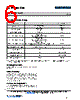
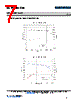
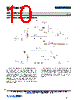
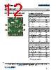
10 / 15 page  SP2T PIN Diode Switch Rev. V1 MSW200x-200 10 10 M/A-COM Technology Solutions Inc. (MACOM) and its affiliates reserve the right to make changes to the product(s) or information contained herein without notice. Visit www.macom.com for additional data sheets and product information. For further information and support please visit: https://www.macom.com/support DS-xxxxxxx 10 SP2T Switch Evaluation Board Schematic The evaluation boards for the MSW200x-200 family of surface mount silicon PIN diode SP2T T-R switches allow the full exercise of each switch for small signal performance analysis, as well as for large signal operation with maximum input signal power of 45 dBm (CW or peak power). Each evaluation board includes the appropriate MSW200x -200 switch, DC blocking capacitors at each RF port and bias decoupling networks at each RF port which allow DC or low frequency control signals to be applied to the switch. Three complementary control signals are required for proper operation. Bias voltages are applied to the TX bias port, RX bias port and the DC bias port to control the state of the switch. A bias voltage of 5 V must be applied to the Ant Bias (pin 3 of multi-pin connector P1) port whenever the switch is in operation. |
|
|
Link URL |
| Does ALLDATASHEET help your business so far? [ DONATE ] |
About Alldatasheet | Advertisement | Contact us | Privacy Policy | Link to Datasheet | Link Exchange | Manufacturer List All Rights Reserved©Alldatasheet.com |
| Russian : Alldatasheetru.com | Korean : Alldatasheet.co.kr | Spanish : Alldatasheet.es | French : Alldatasheet.fr | Italian : Alldatasheetit.com Portuguese : Alldatasheetpt.com | Polish : Alldatasheet.pl | Vietnamese : Alldatasheet.vn Indian : Alldatasheet.in | Mexican : Alldatasheet.com.mx | British : Alldatasheet.co.uk | New Zealand : Alldatasheet.co.nz |
|
Family Site : ic2ic.com |
icmetro.com |
 English ▼
 English
 Chinese
 German
 Japanese
 Russian
 Korean
 Spanish
 French
 Italian
 Portuguese
 Polish
 Vietnamese
 Indian
 Mexican
 British
 New Zealand