|
Electronic Components Datasheet Search |
|
|
Electronic Components Datasheet Search |
|
AD627ARZ-R7 Datasheet(PDF) 21 Page - Analog Devices |
|
|
|||||||||||||||||||||||||||||
AD627ARZ-R7 Datasheet(HTML) 21 Page - Analog Devices |
|
|
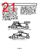
21 / 25 page  AD627 Data Sheet Rev. E | Page 20 of 24 LAYOUT AND GROUNDING The use of ground planes is recommended to minimize the impedance of ground returns (and hence, the size of dc errors). To isolate low level analog signals from a noisy digital environment, many data acquisition components have separate analog and digital ground returns (see Figure 47). Return all ground pins from mixed-signal components, such as analog-to-digital converters, through the high quality analog ground plane. Digital ground lines of mixed-signal components should also be returned through the analog ground plane. This may seem to break the rule of separating analog and digital grounds; however, in general, there is also a requirement to keep the voltage difference between digital and analog grounds on a converter as small as possible (typically, <0.3 V). The increased noise, caused by the digital return currents of the converter flowing through the analog ground plane, is generally negligible. To maximize isolation between analog and digital, connect the ground planes back at the supplies. If there is only one power supply available, it must be shared by both digital and analog circuitry. Figure 48 shows how to minimize interference between the digital and analog circuitry. As in the previous case, use separate analog and digital ground planes or use reasonably thick traces as an alternative to a digital ground plane. Connect the ground planes at the ground pin of the power supply. Run separate traces (or power planes) from the power supply to the supply pins of the digital and analog circuits. Ideally, each device should have its own power supply trace, but they can be shared by multiple devices if a single trace is not used to route current to both digital and analog circuitry. VIN1 VDD VIN2 AD627 7 4 4 1 6 14 3 5 3 6 2 AD627 AD7892-2 0.1µF 0.1µF 0.1µF 0.1µF ANALOG POWER SUPPLY +5V –5V GND AGND VDD MICRO- PROCESSOR AGND ADC DGND DIGITAL POWER SUPPLY +5V GND 12 Figure 47. Optimal Grounding Practice for a Bipolar Supply Environment with Separate Analog and Digital Supplies 0.1µF VIN VDD AD627 7 4 4 1 5 3 6 2 AD7892-2 0.1µF 0.1µF AGND VDD MICRO- PROCESSOR DGND ADC DGND POWER SUPPLY 5V GND 12 Figure 48. Optimal Ground Practice in a Single-Supply Environment |
|
|
Link URL |
| Does ALLDATASHEET help your business so far? [ DONATE ] |
About Alldatasheet | Advertisement | Contact us | Privacy Policy | Link to Datasheet | Link Exchange | Manufacturer List All Rights Reserved©Alldatasheet.com |
| Russian : Alldatasheetru.com | Korean : Alldatasheet.co.kr | Spanish : Alldatasheet.es | French : Alldatasheet.fr | Italian : Alldatasheetit.com Portuguese : Alldatasheetpt.com | Polish : Alldatasheet.pl | Vietnamese : Alldatasheet.vn Indian : Alldatasheet.in | Mexican : Alldatasheet.com.mx | British : Alldatasheet.co.uk | New Zealand : Alldatasheet.co.nz |
|
Family Site : ic2ic.com |
icmetro.com |
 English ▼
 English
 Chinese
 German
 Japanese
 Russian
 Korean
 Spanish
 French
 Italian
 Portuguese
 Polish
 Vietnamese
 Indian
 Mexican
 British
 New Zealand