|
Electronic Components Datasheet Search |
|
|
Electronic Components Datasheet Search |
|
AD627ARZ-R7 Datasheet(PDF) 23 Page - Analog Devices |
|
|
|||||||||||||||||||||||||||||
AD627ARZ-R7 Datasheet(HTML) 23 Page - Analog Devices |
|
|
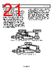
23 / 25 page  AD627 Data Sheet Rev. E | Page 22 of 24 APPLICATIONS CIRCUITS CLASSIC BRIDGE CIRCUIT Figure 50 shows the AD627 configured to amplify the signal from a classic resistive bridge. This circuit works in dual-supply mode or single-supply mode. Typically, the same voltage that powers the instrumentation amplifiers excites the bridge. Connecting the bottom of the bridge to the negative supply of the instrumentation amplifiers (usually 0 V, −5 V, −12 V, or −15 V), sets up an input common-mode voltage that is optimally located midway between the supply voltages. It is also appropriate to set the voltage on the REF pin to midway between the supplies, especially if the input signal is bipolar. However, the voltage on the REF pin can be varied to suit the application. For example, the REF pin is tied to the VREF pin of an analog-to-digital converter (ADC) whose input range is (VREF ± VIN). With an available output swing on the AD627 of (−VS + 100 mV) to (+VS − 150 mV), the maximum programmable gain is simply this output range divided by the input range. VOUT VDIFF +VS –VS VREF 0.1µF 0.1µF AD627 RG = 200kΩ GAIN–5 Figure 50. Classic Bridge Circuit 4 mA TO 20 mA SINGLE-SUPPLY RECEIVER Figure 51 shows how a signal from a 4 mA to 20 mA transducer can be interfaced to the ADuC812, a 12-bit ADC with an embedded microcontroller. The signal from a 4 mA to 20 mA transducer is single-ended, which initially suggests the need for a simple shunt resistor to convert the current to a voltage at the high impedance analog input of the converter. However, any line resistance in the return path (to the transducer) adds a current dependent offset error; therefore, the current must be sensed differentially. In this example, a 24.9 Ω shunt resistor generates a maximum differential input voltage to the AD627 of between 100 mV (for 4 mA in) and 500 mV (for 20 mA in). With no gain resistor present, the AD627 amplifies the 500 mV input voltage by a factor of 5, to 2.5 V, the full-scale input voltage of the ADC. The zero current of 4 mA corresponds to a code of 819 and the LSB size is 4.88 μA. THERMOCOUPLE AMPLIFIER Because the common-mode input range of the AD627 extends 0.1 V below ground, it is possible to measure small differential signals that have a low, or no, common-mode component. Figure 51 shows a thermocouple application where one side of the J-type thermocouple is grounded. Over a temperature range from −200°C to +200°C, the J-type thermocouple delivers a voltage ranging from −7.890 mV to +10.777 mV. A programmed gain on the AD627 of 100 (RG = 2.1 kΩ) and a voltage on the AD627 REF pin of 2 V result in the output voltage of the AD627 ranging from 1.110 V to 3.077 V relative to ground. For a different input range or different voltage on the REF pin, it is important to verify that the voltage on Internal Node A1 (see Figure 37) is not driven below ground. This can be checked using the equations in the Input Range Limitations in Single-Supply Applications section. VOUT 5V VREF 0.1µF AD627 RG 2.1kΩ J-TYPE THERMOCOUPLE REF Figure 51. Amplifying Bipolar Signals with Low Common-Mode Voltage |
|
|
Link URL |
| Does ALLDATASHEET help your business so far? [ DONATE ] |
About Alldatasheet | Advertisement | Contact us | Privacy Policy | Link to Datasheet | Link Exchange | Manufacturer List All Rights Reserved©Alldatasheet.com |
| Russian : Alldatasheetru.com | Korean : Alldatasheet.co.kr | Spanish : Alldatasheet.es | French : Alldatasheet.fr | Italian : Alldatasheetit.com Portuguese : Alldatasheetpt.com | Polish : Alldatasheet.pl | Vietnamese : Alldatasheet.vn Indian : Alldatasheet.in | Mexican : Alldatasheet.com.mx | British : Alldatasheet.co.uk | New Zealand : Alldatasheet.co.nz |
|
Family Site : ic2ic.com |
icmetro.com |
 English ▼
 English
 Chinese
 German
 Japanese
 Russian
 Korean
 Spanish
 French
 Italian
 Portuguese
 Polish
 Vietnamese
 Indian
 Mexican
 British
 New Zealand