|
Electronic Components Datasheet Search |
|
|
Electronic Components Datasheet Search |
|
A25LS512A Datasheet(PDF) 5 Page - AMIC Technology |
|
|
|||||||||||||||||||||||||||||
A25LS512A Datasheet(HTML) 5 Page - AMIC Technology |
|
|
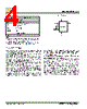
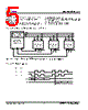
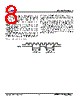
5 / 43 page  A25LS512A Series (November, 2014, Version 1.1) 4 AMIC Technology Corp. SPI MODES These devices can be driven by a microcontroller with its SPI peripheral running in either of the two following modes: – CPOL=0, CPHA=0 – CPOL=1, CPHA=1 For these two modes, input data is latched in on the rising edge of Serial Clock (C), and output data is available from the falling edge of Serial Clock (C). The difference between the two modes, as shown in Figure 2, is the clock polarity when the bus master is in Stand-by mode and not transferring data: – C remains at 0 for (CPOL=0, CPHA=0) – C remains at 1 for (CPOL=1, CPHA=1) Figure 1. Bus Master and Memory Devices on the SPI Bus Bus Master (ST6, ST7, ST9, ST10, Other) SPI Interface with (CPOL, CPHA) = (0, 0) or (1, 1) CS3 CS2 CS1 SPI Memory Device CDO DIO S W HOLD SPI Memory Device S W HOLD SPI Memory Device S W HOLD SDI SDO SCK CDO DIO CDO DIO Note: The Write Protect ( W ) and Hold (HOLD ) signals should be driven, High or Low as appropriate. Figure 2. SPI Modes Supported MSB MSB C C DIO DO 00 1 1 CPOL CPHA |
|
Link URL |
| Does ALLDATASHEET help your business so far? [ DONATE ] |
About Alldatasheet | Advertisement | Contact us | Privacy Policy | Link to Datasheet | Link Exchange | Manufacturer List All Rights Reserved©Alldatasheet.com |
| Russian : Alldatasheetru.com | Korean : Alldatasheet.co.kr | Spanish : Alldatasheet.es | French : Alldatasheet.fr | Italian : Alldatasheetit.com Portuguese : Alldatasheetpt.com | Polish : Alldatasheet.pl | Vietnamese : Alldatasheet.vn Indian : Alldatasheet.in | Mexican : Alldatasheet.com.mx | British : Alldatasheet.co.uk | New Zealand : Alldatasheet.co.nz |
|
Family Site : ic2ic.com |
icmetro.com |
 English ▼
 English
 Chinese
 German
 Japanese
 Russian
 Korean
 Spanish
 French
 Italian
 Portuguese
 Polish
 Vietnamese
 Indian
 Mexican
 British
 New Zealand