|
Electronic Components Datasheet Search |
|
|
Electronic Components Datasheet Search |
|
UPD6600AGS Datasheet(PDF) 5 Page - NEC |
|
|
|||||||||||||||||||||||||||||
UPD6600AGS Datasheet(HTML) 5 Page - NEC |
|
|
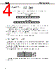
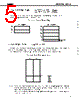
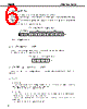
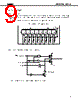
5 / 36 page  µPD6124A, 6600A 5 3. PROGRAM MEMORY (ROM) ……… 512 STEPS × 10 BITS : µPD6600A 1002 STEPS × 10 BITS : µPD6124A The program memory (ROM) is configured in 10 bits steps. It is addressed by the program counter. Program and table data are stored in the program memory. Figure 3-1. Program Memory Map 000H 0FFH 100H 1FFH Test program area PD6124A (b) PD6600A (a) 000H 0FFH 100H 1FFH 200H 2FFH 300H 3E9H 3EAH 3FFH µ µ 4. DATA MEMORY (RAM) ……… 32 WORDS × 5 BITS The data memory is a RAM of 32 words × 5 bits. The data memory stores processing data. In some cases, the data memory is processed in 8-bit units. R0 may be used as the data pointer for the ROM. After power application, the RAM will be undefined. The RAM retains the previous data on reset. Figure 4-1. Data Memory Organization 1 R0 0 RF RB RC SP–3 SP–2 SP–1 SP–0 .. . .. . Caution Avoid using the RAM areas RD, RE, and RF in a CALL routine as much as possible because these areas are also used as stack memory areas (to prevent program hang-up in case the value of the SP is destroyed due to some reason such as noise). When using these RAM areas as general-purpose RAM areas, be sure to include stack pointer checking in the main routine. 0 0 1 1 0 0 1 1 |
|
Link URL |
| Does ALLDATASHEET help your business so far? [ DONATE ] |
About Alldatasheet | Advertisement | Contact us | Privacy Policy | Link to Datasheet | Link Exchange | Manufacturer List All Rights Reserved©Alldatasheet.com |
| Russian : Alldatasheetru.com | Korean : Alldatasheet.co.kr | Spanish : Alldatasheet.es | French : Alldatasheet.fr | Italian : Alldatasheetit.com Portuguese : Alldatasheetpt.com | Polish : Alldatasheet.pl | Vietnamese : Alldatasheet.vn Indian : Alldatasheet.in | Mexican : Alldatasheet.com.mx | British : Alldatasheet.co.uk | New Zealand : Alldatasheet.co.nz |
|
Family Site : ic2ic.com |
icmetro.com |
 English ▼
 English
 Chinese
 German
 Japanese
 Russian
 Korean
 Spanish
 French
 Italian
 Portuguese
 Polish
 Vietnamese
 Indian
 Mexican
 British
 New Zealand