|
Electronic Components Datasheet Search |
|
|
Electronic Components Datasheet Search |
|
ADA4558WHCPZ-R7 Datasheet(PDF) 4 Page - Analog Devices |
|
|
|||||||||||||||||||||||||||||
ADA4558WHCPZ-R7 Datasheet(HTML) 4 Page - Analog Devices |
|
|
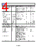
4 / 12 page  ADA4558 Data Sheet Rev. 0 | Page 4 of 12 Parameter Symbol Test Conditions/Comments Min Typ Max Unit EXTERNAL TEMPERATURE SENSOR Valid Temperature Range −50 +165 °C External Temperature Sensor Accuracy Two calibration points using a PT1000 sensor −0.5 +0.5 °C One calibration point using a PT1000 sensor −2 +2 °C Gain Setting Accuracy −2 ±0.2 +2 % LIN INPUT AND OUTPUT STAGE Compliant with LIN Specification 2.1 Voltage Voltage range over which LIN is functional 6 18 V Baud Rate 1 20 kbps Current Limit for Driver (LIN Bus Dominant State) ILIN_DOM_MAX Pulled to maximum VDD12 40 200 mA Driver Off ILIN_PASS_REC 8 V < VDD12 < 18 V, VLIN ≥ VDD12 20 μA Input Leakage ILIN_PAS_DOM VLIN = 0 V −1 mA LIN Pin Current While Ground Disconnected ILIN_NO_GND VDD12 = 12 V, control unit disconnected from ground −1 +1 mA While Battery Disconnected ILIN_NO_BAT VDD12 disconnected, 0 V < VLIN < 18 V 30 μA LIN Receiver Dominant State VLIN_DOM 40 % VDD12 Recessive State VLIN_REC 60 % VDD12 Center Voltage VLIN_CNT 47.5 50 52.5 % VDD12 Hysteresis Voltage VHYS 17.5 % VDD12 Slave Termination Resistance RSLAVE 21 25 34 kΩ LIN RECEIVER TIMING PARAMETERS Propagation Delay of Receiver tRX_PD 6 µs Symmetry of Receiver Propagation Delay tRX_SYM Rising edge with the respect to falling edge −2 +2 µs LIN DRIVER TIMING PARAMETERS Bus load conditions (CBUS, RBUS): 1 nF and 1 kΩ; 6.8 nF and 660 Ω; 10 nF and 500 Ω Duty Cycle 1 D1 For proper operation at 20 kbps 0.396 Duty Cycle 2 D2 For proper operation at 20 kbps 0.581 Duty Cycle 3 D3 For proper operation at 10.4 kbps 0.417 Duty Cycle 4 D4 For proper operation at 10.4 kbps 0.590 ADC Measurement Time To valid reading 120 µs LIN SLEEP/WAKE-UP Force sleep mode by sending a diagnostic master request frame (frame identifier = 0x3C, with the first data byte equal to 0x00); sleep mode is also entered if there is no activity on the LIN bus for a certain time Auto Sleep Enable Time Wake-up occurs if a recessive to dominant transition on the LIN bus is followed by a dominant level on the LIN bus maintained for a certain time (minimum dominant time), followed by a dominant to recessive transition; the dominant to recessive transition wakes up the device 4 sec Minimum Dominant Time 150 µs |
|
|
Link URL |
| Does ALLDATASHEET help your business so far? [ DONATE ] |
About Alldatasheet | Advertisement | Contact us | Privacy Policy | Link to Datasheet | Link Exchange | Manufacturer List All Rights Reserved©Alldatasheet.com |
| Russian : Alldatasheetru.com | Korean : Alldatasheet.co.kr | Spanish : Alldatasheet.es | French : Alldatasheet.fr | Italian : Alldatasheetit.com Portuguese : Alldatasheetpt.com | Polish : Alldatasheet.pl | Vietnamese : Alldatasheet.vn Indian : Alldatasheet.in | Mexican : Alldatasheet.com.mx | British : Alldatasheet.co.uk | New Zealand : Alldatasheet.co.nz |
|
Family Site : ic2ic.com |
icmetro.com |
 English ▼
 English
 Chinese
 German
 Japanese
 Russian
 Korean
 Spanish
 French
 Italian
 Portuguese
 Polish
 Vietnamese
 Indian
 Mexican
 British
 New Zealand