|
Electronic Components Datasheet Search |
|
|
Electronic Components Datasheet Search |
|
ADA4558WHCPZ-R7 Datasheet(PDF) 7 Page - Analog Devices |
|
|
|||||||||||||||||||||||||||||
ADA4558WHCPZ-R7 Datasheet(HTML) 7 Page - Analog Devices |
|
|
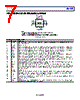
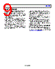
7 / 12 page  Data Sheet ADA4558 Rev. 0 | Page 7 of 12 PIN CONFIGURATION AND FUNCTION DESCRIPTIONS 14 13 12 1 3 4 TNEG 15 ISINK TPOS RREFN 11 VREG DVDD TESTD 2 DGND SWDIO 5 SWCLK NOTES 1. NIC = NOT INTERNALLY CONNECTED. THIS PIN IS NOT INTERNALLY CONNECTED. CONNECT NIC TO THE GROUND PLANE. 2. CONNECT THE EXPOSED PAD OF THE LFCSP PACKAGE TO THE ANALOG GROUND PLANE. ENSURE THAT AGND IS CONNECTED TO DGND AND LINGND AT A SINGLE POINT ON THE PCB. ADA4558 TOP VIEW (Not to Scale) Figure 2. Pin Configuration Table 4. Pin Function Descriptions Pin No. Mnemonic Description 1 DVDD 1.8 V Low Dropout (LDO) Digital Supply. Add a 0.1 μF capacitor placed as close to Pin 1 as possible between DVDD and the DGND plane. 2 DGND Digital Ground. 3 TESTD Test Pin. Analog Devices, Inc., uses this pin at the production test. Connect TESTD to the DGND plane in the application. 4 SWDIO Test Pin. Analog Devices uses this pin at the production test. Connect SWDIO to the DGND plane in the application. 5 SWCLK Test Pin. Analog Devices uses this pin at the production test. Connect SWCLK to the DGND plane in the application. 6 NIC Not Internally Connected. This pin is not internally connected. Connect NIC to the ground plane. 7 VNEG Negative Input. Pin 7 is the negative input to the PGA from the external resistive bridge. 8 TEST1 Test Pin. Analog Devices uses this pin at the production test. Connect TEST1 to the AGND plane in the application. 9 VPOS Positive Input. Pin 9 is the positive input to the PGA from an external resistive bridge. 10 TEST2 Test Pin. Analog Devices uses this pin at the production test. Connect TEST2 to the AGND plane in the application. 11 VREG Regulated 4.0 V Output. Pin 11 drives the top of the external bridge. Add a 0.1 μF capacitor between VREG and the AGND plane, placed as close to the VREG pin as possible. 12 RREFN Reference Resistor. Pin 12 is the reference resistor for the external temperature sensor sense connection. Connect Pin 12 to ground when there is no external temperature sensor. 13 TPOS External Temperature Positive Input. Connect Pin 13 to ground when there is no external temperature sensor. 14 TNEG External Temperature Sensor Negative Input. Connect Pin 14 to ground when there is no external temperature sensor. 15 ISINK Current Sink. Pin 15 drives the external temperature sensor. Connect Pin 15 to ground when there is no external temperature sensor. 16 AGND Analog Ground. 17 VDD12 Supply. Connect the 12 V battery supply to this pin. Decouple VDD12 with a 1 µF capacitor. A 100 nF capacitor can be used only when a 1 µF capacitor to ground is placed on the anode of the diode on the module battery supply. 18 LIN2 Not in Use. The LIN2 function is not in use. Connect LIN2 to the LIN pin. 19 LIN LIN Compliant Interface. All communication to and from the IC is via the LIN pin. Connect a LIN capacitor to ground on this pin, per the LIN specification. 20 LINGND Local LIN Ground. EPAD Exposed Pad. Connect the exposed pad of the LFCSP to the analog ground plane. Ensure that AGND is connected to DGND and LINGND at a single point on the PCB. |
|
|
Link URL |
| Does ALLDATASHEET help your business so far? [ DONATE ] |
About Alldatasheet | Advertisement | Contact us | Privacy Policy | Link to Datasheet | Link Exchange | Manufacturer List All Rights Reserved©Alldatasheet.com |
| Russian : Alldatasheetru.com | Korean : Alldatasheet.co.kr | Spanish : Alldatasheet.es | French : Alldatasheet.fr | Italian : Alldatasheetit.com Portuguese : Alldatasheetpt.com | Polish : Alldatasheet.pl | Vietnamese : Alldatasheet.vn Indian : Alldatasheet.in | Mexican : Alldatasheet.com.mx | British : Alldatasheet.co.uk | New Zealand : Alldatasheet.co.nz |
|
Family Site : ic2ic.com |
icmetro.com |
 English ▼
 English
 Chinese
 German
 Japanese
 Russian
 Korean
 Spanish
 French
 Italian
 Portuguese
 Polish
 Vietnamese
 Indian
 Mexican
 British
 New Zealand