|
Electronic Components Datasheet Search |
|
|
Electronic Components Datasheet Search |
|
ISL8117DEMO2Z Datasheet(PDF) 9 Page - Renesas Technology Corp |
|
|
|||||||||||||||||||||||||||||
ISL8117DEMO2Z Datasheet(HTML) 9 Page - Renesas Technology Corp |
|
|
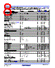
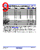
9 / 24 page  ISL8117 FN8666 Rev 4.00 Page 9 of 24 Apr 19, 2018 PWM GATE DRIVER Source Current IGSRC 2000 mA Sink Current IGSNK 2000 mA Upper Drive Pull-Up RUG_UP VCC5V = 5.0V 1.5 Ω Upper Drive Pull-Down RUG_DN VCC5V = 5.0V 1.5 Ω Lower Drive Pull-Up RLG_UP VCC5V = 5.0V 1.0 Ω Lower Drive Pull-Down RLG_DN VCC5V = 5.0V 0.8 Ω Upper Drive Rise Time tGR_UP COUT = 1000pF 9.0 ns Upper Drive Fall Time tGF_UP COUT = 1000pF 8.0 ns Lower Drive Rise Time tGR_DN COUT = 1000pF 7.0 ns Lower Drive Fall Time tGF_DN COUT = 1000pF 6.1 ns OVERVOLTAGE PROTECTION OVP Threshold VOVTH 116 121 127 % OVERCURRENT PROTECTION OC Set Current Source IOCSET-CS LGATE/OCS = 0V 9 10.5 11.5 µA OVER-TEMPERATURE Over-Temperature Shutdown TOT-TH 160 °C Over-Temperature Hysteresis TOT-HYS 15 °C NOTES: 6. In normal operation, where the device is supplied with voltage on the VIN pin, the VCC5V pin provides a 5V output capable of 75mA (min). When the device is supplied by an external 5V supply on the EXTBIAS pin, the internal LDO regulator is disabled. The voltage at VCC5V should not exceed the voltage at VIN at any time. (Refer to “Pin Descriptions” on page 3 for more details.) 7. This is the total shutdown current with VIN = 5.6V and 60V. 8. Operating current is the supply current consumed when the device is active but not switching. It does not include gate drive current. 9. Parameters with MIN and/or MAX limits are 100% tested at +25°C, unless otherwise specified. Temperature limits established by characterization and are not production tested. 10. Threshold voltage at PHASE pin for turning off the bottom MOSFET during DEM. 11. When soft-start time is less than 4.5ms, tPGR increases. With internal soft-start (the fastest soft-start time), tPGR increases close to its max limit 5ms. Electrical Specifications Recommended operating conditions unless otherwise noted. Refer to “Block Diagram” on page 5 and “Typical Application Schematics” on page 6. VIN = 4.5V to 60V, or VCC5V = 5V ±10%, C_VCC5V = 4.7µF, TA = -40°C to +125°C, Typical values are at TA = +25°C, unless otherwise specified. Boldface limits apply across the operating temperature range, -40°C to +125°C. (Continued) PARAMETER SYMBOL TEST CONDITIONS MIN (Note 9)TYP MAX (Note 9)UNIT |
|
|
Link URL |
| Does ALLDATASHEET help your business so far? [ DONATE ] |
About Alldatasheet | Advertisement | Contact us | Privacy Policy | Link to Datasheet | Link Exchange | Manufacturer List All Rights Reserved©Alldatasheet.com |
| Russian : Alldatasheetru.com | Korean : Alldatasheet.co.kr | Spanish : Alldatasheet.es | French : Alldatasheet.fr | Italian : Alldatasheetit.com Portuguese : Alldatasheetpt.com | Polish : Alldatasheet.pl | Vietnamese : Alldatasheet.vn Indian : Alldatasheet.in | Mexican : Alldatasheet.com.mx | British : Alldatasheet.co.uk | New Zealand : Alldatasheet.co.nz |
|
Family Site : ic2ic.com |
icmetro.com |
 English ▼
 English
 Chinese
 German
 Japanese
 Russian
 Korean
 Spanish
 French
 Italian
 Portuguese
 Polish
 Vietnamese
 Indian
 Mexican
 British
 New Zealand