|
Electronic Components Datasheet Search |
|
|
Electronic Components Datasheet Search |
|
ADL5206ACPZ-R7 Datasheet(PDF) 24 Page - Analog Devices |
|
|
|||||||||||||||||||||||||||||
ADL5206ACPZ-R7 Datasheet(HTML) 24 Page - Analog Devices |
|
|
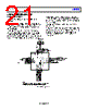
24 / 25 page  ADL5206 Data Sheet Rev. 0 | Page 24 of 25 ADC INTERFACING A typical data acquisition system using the ADL5206 together with an antialiasing filter and an ADC is shown in Figure 63. The main role of the filter after the amplifier is for attenuating the broadband noise and out of band harmonics generated by the amplifier. Component values for a 500 MHz acquisition bandwidth are listed in Table 13. Without this filter, the out of band noise and distortion components alias back into the Nyquist band, resulting in a reduction of signal-to-noise ratio. The design of the filter preceding the ADL5206 amplifier is more specific to the system rejection requirements for the acquisition system. C4 R1A R1B L3A L1A L3B L1B VCM C2B C2A ADC AMP FILTER Figure 63. ADC Interface (One of Two Channels Shown) Table 13. Component Values for a 500 MHz Acquisition System Component Value Description/Comments Amplifier ½ ADL5206 One channel L1A, L1B 22 nH Q ≥ 50 at 500 MHz C2A, C2B 6.8 pF Final value depends on PCB parasitics L3A, L3B 22 nH Q ≥ 50 at 500 MHz C4 1.5 pF Final value depends on PCB parasitics R1A, R1B 10 Ω Not applicable ADC ½ AD9680 One channel, input impedance set to 100 Ω NOISE FIGURE vs. GAIN SETTING Because of the architecture of the ADL5206, the noise figure does not degrade significantly for the first 10 dB of gain reduction from the maximum gain setting. The noise figure increases by 0.5 dB only during the first 10 dB of gain reduction. The noise figure changes by 7 dB over the 30 dB gain range. 0 5 10 15 20 25 30 35 40 45 GAIN (dB) ADL5206 AT 700MHz 5V HIGH PERFORMANCE REGULAR ATTENUATOR AMPLIFIER CASCADE –10 –5 0 5 10 15 20 25 30 32 Figure 64. Noise Figure vs. Gain |
|
|
Link URL |
| Does ALLDATASHEET help your business so far? [ DONATE ] |
About Alldatasheet | Advertisement | Contact us | Privacy Policy | Link to Datasheet | Link Exchange | Manufacturer List All Rights Reserved©Alldatasheet.com |
| Russian : Alldatasheetru.com | Korean : Alldatasheet.co.kr | Spanish : Alldatasheet.es | French : Alldatasheet.fr | Italian : Alldatasheetit.com Portuguese : Alldatasheetpt.com | Polish : Alldatasheet.pl | Vietnamese : Alldatasheet.vn Indian : Alldatasheet.in | Mexican : Alldatasheet.com.mx | British : Alldatasheet.co.uk | New Zealand : Alldatasheet.co.nz |
|
Family Site : ic2ic.com |
icmetro.com |
 English ▼
 English
 Chinese
 German
 Japanese
 Russian
 Korean
 Spanish
 French
 Italian
 Portuguese
 Polish
 Vietnamese
 Indian
 Mexican
 British
 New Zealand