|
Electronic Components Datasheet Search |
|
|
Electronic Components Datasheet Search |
|
EM62100AGH Datasheet(PDF) 18 Page - ELAN Microelectronics Corp |
|
|
|||||||||||||||||||||||||||||
EM62100AGH Datasheet(HTML) 18 Page - ELAN Microelectronics Corp |
|
|
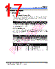
18 / 60 page  EM62100 65 COM/132 SEG STN LCD Driver 12 • ••• Product Specification (V1.1) 09.13.2005 (This specification is subject to change without further notice) 6.1.3 Serial Interface When the EM62100 is active (CS1B=”L” and CS2=”H”), the serial data input (SI) and the serial clock input (SCL) can be received. The serial data can be read from the SI pin in the rising edge of the serial clocks D7, D6 through D0, in this order. This data is converted to 8 bits parallel data in the rising edge of the 8th serial clock for processing. The RS input is used to determine whether the serial data input is display data (RS=”H”) or command data (RS=”L”). The RS input is read and used for detection every 8th rising edge of the serial clock after the chip becomes active. Figure 2 is a serial interface signal chart. 1 2 3 4 5 6 7 8 9 10 11 12 SCL D7 D6 D4 D5 D6 D6 D0 D1 D2 D3 D4 D5 SI CS CS1B = "L" and CS2 = "H" RS Fig. 2 NOTE 1. When the chip is not active, the shift registers and counter are reset to their initial states. 2. Reading is not possible while in serial interface mode. 3. Caution is required on the SCL signal when it comes to line-end reflections and external noise. It is recommended that operation be rechecked on the actual equipment. 6.1.4 Chip Select The EM62100 has two chip select terminals: CS1B and CS2. The MPU interface or the serial interface is enabled only when CS1B=”L” and CS2=”H”. When the chip select is non-active D0 to D7 enter high impedance and the RS, RDB, and WRB inputs are inactive. When the serial interface is selected, the shift register and the counter are reset. |
|
Link URL |
| Does ALLDATASHEET help your business so far? [ DONATE ] |
About Alldatasheet | Advertisement | Contact us | Privacy Policy | Link to Datasheet | Link Exchange | Manufacturer List All Rights Reserved©Alldatasheet.com |
| Russian : Alldatasheetru.com | Korean : Alldatasheet.co.kr | Spanish : Alldatasheet.es | French : Alldatasheet.fr | Italian : Alldatasheetit.com Portuguese : Alldatasheetpt.com | Polish : Alldatasheet.pl | Vietnamese : Alldatasheet.vn Indian : Alldatasheet.in | Mexican : Alldatasheet.com.mx | British : Alldatasheet.co.uk | New Zealand : Alldatasheet.co.nz |
|
Family Site : ic2ic.com |
icmetro.com |
 English ▼
 English
 Chinese
 German
 Japanese
 Russian
 Korean
 Spanish
 French
 Italian
 Portuguese
 Polish
 Vietnamese
 Indian
 Mexican
 British
 New Zealand