|
Electronic Components Datasheet Search |
|
|
Electronic Components Datasheet Search |
|
EM62100AGH Datasheet(PDF) 30 Page - ELAN Microelectronics Corp |
|
|
|||||||||||||||||||||||||||||
EM62100AGH Datasheet(HTML) 30 Page - ELAN Microelectronics Corp |
|
|
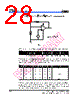
30 / 60 page  EM62100 65 COM/132 SEG STN LCD Driver 24 • ••• Product Specification (V1.1) 09.13.2005 (This specification is subject to change without further notice) 6.12.4 High Power Mode The EM62100 built-in power supply circuit has very low power consumption (normal mode: HPMB=“H”). If used for LCD panels with large loads, this low-power power supply may cause the display quality to degrade. When this occurs, setting the HPMB terminal to “L” (high power mode) can improve the display quality. It is recommended that the display be checked on the actual equipment to determine whether or not to use this mode. Moreover, if the improvement to the display is inadequate even after the high power mode has been set, then it is a must to add a Command Sequence when the Built-in Power Supply is turned OFF. To turn off the built-in power supply, follow the command sequence as shown below, wherein you have to turn it off after making the system enter the standby mode. 6.12.5 Reference Power Supply Circuit for Driving the LCD Panel V OUT CAP4+ CAP2+ CAP2- CAP1+ CAP1- CAP3+ V REF V 0 V 1 V 2 V 3 V 4 V SS C1 C1 C1 C2 C2 C2 C2 C2 C1 M/S V DD C2 C2 C2 C2 C2 Using only voltage follower Not using internal LCD power supply circuits Using all LCD power circuits (Voltage booster, regulator and follower) The following diagram illustrates using 4X boosting circuit and internal regulator resistors, IRS =1 Not using voltage booster circuits The following circuit diagram illustrates using external regulator resistors, IRS = 0 External Power Supply Ra C2 C2 C2 C2 C2 External Power Supply External Power Supply Value of External Capacitance µF ITEM Value C2 0.1 - 2.2 C1 1.0 - 4.7 M/S M/S M/S CAP4+ CAP2+ CAP2- CAP1+ CAP1- CAP3+ CAP4+ CAP2+ CAP2- CAP1+ CAP1- CAP3+ CAP4+ CAP2+ CAP2- CAP1+ CAP1- CAP3+ V OUT V 0 V 1 V 2 V 3 V 4 V SS V DD V OUT V 0 V 1 V 2 V 3 V 4 V SS V DD V OUT V 0 V 1 V 2 V 3 V 4 V SS V DD V REF V REF V REF Fig.11 |
|
Link URL |
| Does ALLDATASHEET help your business so far? [ DONATE ] |
About Alldatasheet | Advertisement | Contact us | Privacy Policy | Link to Datasheet | Link Exchange | Manufacturer List All Rights Reserved©Alldatasheet.com |
| Russian : Alldatasheetru.com | Korean : Alldatasheet.co.kr | Spanish : Alldatasheet.es | French : Alldatasheet.fr | Italian : Alldatasheetit.com Portuguese : Alldatasheetpt.com | Polish : Alldatasheet.pl | Vietnamese : Alldatasheet.vn Indian : Alldatasheet.in | Mexican : Alldatasheet.com.mx | British : Alldatasheet.co.uk | New Zealand : Alldatasheet.co.nz |
|
Family Site : ic2ic.com |
icmetro.com |
 English ▼
 English
 Chinese
 German
 Japanese
 Russian
 Korean
 Spanish
 French
 Italian
 Portuguese
 Polish
 Vietnamese
 Indian
 Mexican
 British
 New Zealand