|
Electronic Components Datasheet Search |
|
|
Electronic Components Datasheet Search |
|
EM62100AGH Datasheet(PDF) 13 Page - ELAN Microelectronics Corp |
|
|
|||||||||||||||||||||||||||||
EM62100AGH Datasheet(HTML) 13 Page - ELAN Microelectronics Corp |
|
|
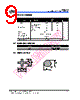
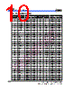
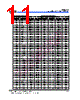
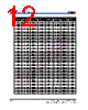
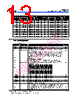
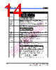
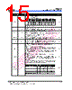
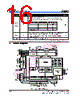
13 / 60 page  EM62100 65 COM/132 SEG STN LCD Driver Product Specification (V1.1) 09.13.2005 •••• 7 (This specification is subject to change without further notice) Coordinate Coordinate Pad No. Pad Name X Y Pad No. Pad Name X Y 289 COM36 -3575.0 388.0 301 COM46 -3988.0 150.0 290 COM37 -3625.0 388.0 302 COM47 -3988.0 100.0 291 COM38 -3675.0 388.0 303 COM48 -3988.0 50.0 292 COM39 -3725.0 388.0 304 COM49 -3988.0 0.0 293 COM40 -3775.0 388.0 305 COM50 -3988.0 -50.0 294 COM41 -3825.0 388.0 306 COM51 -3988.0 -100.0 295 NC10 -3875.0 388.0 307 COM52 -3988.0 -150.0 296 NC11 -3988.0 400.0 308 COM53 -3988.0 -200.0 297 COM42 -3988.0 350.0 309 COM54 -3988.0 -250.0 298 COM43 -3988.0 300.0 310 COM55 -3988.0 -300.0 299 COM44 -3988.0 250.0 311 COM56 -3988.0 -350.0 300 COM45 -3988.0 200.0 312 NC12 -3988.0 -400.0 4 Pin Description Table 1 Pin Name I/O Function No. of Pins VDD Power Supply Power supply terminal VCC 8 VSS Power Supply System Ground 12 VEE Power Supply Voltage supply pin for booster circuit. Usually the same voltage level as VDD. 6 Multi-level power supply for the liquid crystal drive. The voltage applied is determined by the liquid crystal cell, and is changed through the use of a resistive voltage divider or by changing the impedance using an Op. Amp. Voltage levels are determined based on V0, and must maintain the relative magnitudes shown below. V0 V1 V2 V3 V4 VSS Master operation: When the power supply is turned ON, the internal power supply circuits produce the V1 to V4 voltages shown below. The voltage settings are selected using the LCD bias set command. V0 V1 V2 V3 V4 Power Supply LCD bias V1 V2 V3 V4 1/4 bias 3/4V0 2/4V0 2/4V0 1/4V0 1/5 bias 4/5V0 3/5V0 2/5V0 1/5V0 1/6 bias 5/6V0 4/6V0 2/6V0 1/6V0 1/7 bias 6/7V0 5/7V0 2/7V0 1/7V0 1/8 bias 7/8V0 6/8V0 2/8V0 1/8V0 1/9 bias 8/9V0 7/9V0 2/9V0 1/9V0 21 CAP1+ O Capacitor 1 positive pin for voltage converter 2 CAP1- O Capacitor 1 negative pin for voltage converter 2 CAP2+ O Capacitor 2 positive pin for voltage converter 2 CAP2- O Capacitor 2 negative pin for voltage converter 3 CAP3+ O Capacitor 3 positive pin for voltage converter 2 CAP4+ O Capacitor 4 positive pin for voltage converter 2 VOUT I/O DC/DC voltage converter input/output pin, connect a capacitor between this terminal and VSS 3 VREF I V0 voltage adjustment pad. Applies voltage between V0 and VSS using a resistive divider. This is only enabled (IRS=“L”) When the V0 voltage regulator internal resistor is not used. When the V0 voltage regulator internal resistor is used (IRS=“H”), this pin must be floating. 1 |
|
Link URL |
| Does ALLDATASHEET help your business so far? [ DONATE ] |
About Alldatasheet | Advertisement | Contact us | Privacy Policy | Link to Datasheet | Link Exchange | Manufacturer List All Rights Reserved©Alldatasheet.com |
| Russian : Alldatasheetru.com | Korean : Alldatasheet.co.kr | Spanish : Alldatasheet.es | French : Alldatasheet.fr | Italian : Alldatasheetit.com Portuguese : Alldatasheetpt.com | Polish : Alldatasheet.pl | Vietnamese : Alldatasheet.vn Indian : Alldatasheet.in | Mexican : Alldatasheet.com.mx | British : Alldatasheet.co.uk | New Zealand : Alldatasheet.co.nz |
|
Family Site : ic2ic.com |
icmetro.com |
 English ▼
 English
 Chinese
 German
 Japanese
 Russian
 Korean
 Spanish
 French
 Italian
 Portuguese
 Polish
 Vietnamese
 Indian
 Mexican
 British
 New Zealand