|
Electronic Components Datasheet Search |
|
|
Electronic Components Datasheet Search |
|
STDEV003ABTR Datasheet(PDF) 12 Page - STMicroelectronics |
|
|
|||||||||||||||||||||||||||||
STDEV003ABTR Datasheet(HTML) 12 Page - STMicroelectronics |
|
|
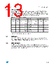
12 / 41 page  Functional description STDVE003A 12/41 across the REXT. The differential output driver provides a typical 10 mA current sink capability, which provides a typical 500 mV voltage drop across a 50 Ω termination resistor. TMDS voltage levels The TMDS interface standard is a signaling method intended for point-to-point communication over a tightly controlled impedance medium. The TMDS standard uses a lower voltage swing than other common communication standards, achieving higher data rates with reduced power consumption while reducing EMI emissions and system susceptibility to noise. The device is capable of detecting differential signals as low as 100 mV within the entire common mode voltage range. 3.2 Operating modes The OE_N input activates a hardware power down mode. When the power down mode is active (OE_N = H), all input and output buffers and internal bias circuitry are powered-off and disabled. Outputs are tri-stated in power-down mode. When exiting power-down mode, there is a delay associated with turning on band-references and input/output buffer circuits. Table 4. OE_N operating modes Input Output Function OE_N IN+ (ports A1, A2 or A3) IN- (ports B1, B2 or B3) OUT+ OUT- LH LH L Active mode LL H L H Active mode H X X Hi-Z Hi-Z Low power mode |
|
Link URL |
| Does ALLDATASHEET help your business so far? [ DONATE ] |
About Alldatasheet | Advertisement | Contact us | Privacy Policy | Link to Datasheet | Link Exchange | Manufacturer List All Rights Reserved©Alldatasheet.com |
| Russian : Alldatasheetru.com | Korean : Alldatasheet.co.kr | Spanish : Alldatasheet.es | French : Alldatasheet.fr | Italian : Alldatasheetit.com Portuguese : Alldatasheetpt.com | Polish : Alldatasheet.pl | Vietnamese : Alldatasheet.vn Indian : Alldatasheet.in | Mexican : Alldatasheet.com.mx | British : Alldatasheet.co.uk | New Zealand : Alldatasheet.co.nz |
|
Family Site : ic2ic.com |
icmetro.com |
 English ▼
 English
 Chinese
 German
 Japanese
 Russian
 Korean
 Spanish
 French
 Italian
 Portuguese
 Polish
 Vietnamese
 Indian
 Mexican
 British
 New Zealand