|
Electronic Components Datasheet Search |
|
|
Electronic Components Datasheet Search |
|
ISL73006SLHDEMO2Z Datasheet(PDF) 5 Page - Renesas Technology Corp |
|
|
|||||||||||||||||||||||||||||
ISL73006SLHDEMO2Z Datasheet(HTML) 5 Page - Renesas Technology Corp |
|
|
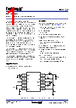
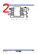
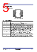
5 / 31 page  R34DS0034EU0101 Rev.1.01 Page 5 Mar 13, 2024 ISL73006SLH Datasheet 2. Pin Information 2.1 Pin Assignments Figure 4. Pin Assignments - Top View 2.2 Pin Descriptions Pin Number Pin Name ESD Circuit Description 1 PGND 3 Power-ground connection. Ground return for the low-side power MOSFET 2 PVIN 1 Power Input. Supplies the power switches of the buck converter. 3EN 2 Enable input. This input is a comparator-type input with a rising threshold of 1.2V. Bypass this pin to the PCB ground plane with a 10nF ceramic capacitor to mitigate SEE. This pin can be tied to a maximum of 5V. 4VCC 2 Linear regulator output from PVIN to provide an internal bias supply rail of up to 5V. Bypass this pin to the PCB ground plane with a 2.2µF ceramic or low ESR Tantalum capacitor for stability, SEE, and noise mitigation. VCC is not intended to bias external circuits 5SLOPE 2 Slope Compensation. Connect a resistor from this pin to GND to externally set the slope compensation. This pin is a current source of 12µA into the external resistor. Connect the SLOPE pin to VCC to use the default internal slope compensation voltage of 1.2V. If not connected to VCC, add a 1nF capacitor from this pin to ground for SEE mitigation. 6FB 2 Error Amplifier inverting input. Connect a resistor divider from VOUT to GND with the midpoint driving the FB pin. 7COMP 2 Error Amplifier output. The external compensation network is connected from this pin to GND. Tie this pin to VCC to use the internal Error Amplifier compensation setup. 10 9 8 7 6 1 2 3 4 5 PGND PVIN EN VCC SLOPE LX PG SGND COMP FB |
|
Link URL |
| Does ALLDATASHEET help your business so far? [ DONATE ] |
About Alldatasheet | Advertisement | Contact us | Privacy Policy | Link to Datasheet | Link Exchange | Manufacturer List All Rights Reserved©Alldatasheet.com |
| Russian : Alldatasheetru.com | Korean : Alldatasheet.co.kr | Spanish : Alldatasheet.es | French : Alldatasheet.fr | Italian : Alldatasheetit.com Portuguese : Alldatasheetpt.com | Polish : Alldatasheet.pl | Vietnamese : Alldatasheet.vn Indian : Alldatasheet.in | Mexican : Alldatasheet.com.mx | British : Alldatasheet.co.uk | New Zealand : Alldatasheet.co.nz |
|
Family Site : ic2ic.com |
icmetro.com |
 English ▼
 English
 Chinese
 German
 Japanese
 Russian
 Korean
 Spanish
 French
 Italian
 Portuguese
 Polish
 Vietnamese
 Indian
 Mexican
 British
 New Zealand