|
Electronic Components Datasheet Search |
|
|
Electronic Components Datasheet Search |
|
ISL73006SLHDEMO2Z Datasheet(PDF) 25 Page - Renesas Technology Corp |
|
|
|||||||||||||||||||||||||||||
ISL73006SLHDEMO2Z Datasheet(HTML) 25 Page - Renesas Technology Corp |
|
|
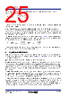
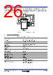
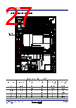
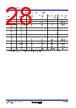
25 / 31 page  R34DS0034EU0101 Rev.1.01 Page 25 Mar 13, 2024 ISL73006SLH Datasheet inductor ripple current and Equation 15 to approximate the output voltage ripple, where ESR is the output capacitor equivalent series resistance. Increasing inductance reduces the ripple current and output voltage ripple; however, the regulator response time to transient load increases. One of the parameters limiting the regulator response to a load transient is the time required to change the inductor current. The response time is the time required to slew the inductor current from its initial level to the transient level. During this interval, the difference between the inductor and transient load current is sourced from or sunk into the output capacitor. Minimizing the response time reduces the amount of transient voltage overshoot and undershoot on the output capacitor. The response time to a transient is different for the transient load on and off. Equation 16 gives the approximate response time to a load step, where ITRAN is the transient load current step, tRISE is the inductor response time to a turn-on load step, and tFALL is the response time to a turn-off load step. The worst-case response time can be during either the load step on or off. Check for transient load response for both turn-on and turn-off at the minimum and maximum load current. 6. Layout Considerations Proper layout of the PCB for the switching converter is important to ensure the switching converter works well to minimize EMI and noise and ensure first pass success of the design. Figure 42 shows the connections of the most critical top-layer components. Note: Capacitors CIN and COUT can each represent multiple physical capacitors. Renesas recommends using a multilayer printed circuit board with buried GND planes. A critical connection is a thermal connection from the package thermal pad to the PCB PGND plane on the top layer. Additionally, connect the IC PGND pins to this GND plane. This connection of the GND pins to the system GND plane ensures a low- impedance path for all return currents and an excellent thermal path to dissipate heat. With this connection made, place the high-frequency ceramic input capacitor(s) across the PVIN and PGND pins. The bulk capacitance can be further away. The power loop comprises the output inductor (LOUT), the output capacitor (COUT), the LX pins, and the PGND pin. Make the power loop as short as possible and the connecting traces direct, short, and wide. An island for the LX node to contain the output inductor is noisy, so keep the voltage feedback trace away from this noisy area. Connect COUT tightly to LOUT and directly as possible to the PGND pins. If implemented, the external compensation loop should also be as short as possible, with the connecting traces to RCOMP and the CCOMP directly between the COMP and SGND pins. The SGND should be connected at 1 point to the PGND plane out of the current flow of the ground plane. A convenient place is under the package to the thermal pad. If implementing internal compensation, tie the COMP pin to VCC as directly as possible, likewise for internal SLOPE selection. The two latter connections are not as critical and can be placed last. (EQ. 14) (EQ. 15) (EQ. 16) IRIPPLE VIN VOUT – fSW L ------------------------------------- VOUT VIN ---------------- = VOUT_RIPPLE IRIPPLE ESR = Load On: tRISE L ITRAN VIN VOUT – -------------------------------- = Load Off: tFALL L ITRAN VOUT --------------------------- = |
|
Link URL |
| Does ALLDATASHEET help your business so far? [ DONATE ] |
About Alldatasheet | Advertisement | Contact us | Privacy Policy | Link to Datasheet | Link Exchange | Manufacturer List All Rights Reserved©Alldatasheet.com |
| Russian : Alldatasheetru.com | Korean : Alldatasheet.co.kr | Spanish : Alldatasheet.es | French : Alldatasheet.fr | Italian : Alldatasheetit.com Portuguese : Alldatasheetpt.com | Polish : Alldatasheet.pl | Vietnamese : Alldatasheet.vn Indian : Alldatasheet.in | Mexican : Alldatasheet.com.mx | British : Alldatasheet.co.uk | New Zealand : Alldatasheet.co.nz |
|
Family Site : ic2ic.com |
icmetro.com |
 English ▼
 English
 Chinese
 German
 Japanese
 Russian
 Korean
 Spanish
 French
 Italian
 Portuguese
 Polish
 Vietnamese
 Indian
 Mexican
 British
 New Zealand