|
Electronic Components Datasheet Search |
|
|
Electronic Components Datasheet Search |
|
ISL73006SLHDEMO2Z Datasheet(PDF) 19 Page - Renesas Technology Corp |
|
|
|||||||||||||||||||||||||||||
ISL73006SLHDEMO2Z Datasheet(HTML) 19 Page - Renesas Technology Corp |
|
|
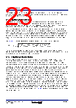
19 / 31 page  R34DS0034EU0101 Rev.1.01 Page 19 Mar 13, 2024 ISL73006SLH Datasheet 5. Theory of Operation 5.1 Description of Features The ISL73006SLH is a Radiation Hardened by design buck converter using constant frequency peak current mode control architecture for fast loop transient response with a 3V to 18V input voltage regulating down to a minimum 0.6V output voltage adjusted using external resistors. The ISL73006SLH is capable of ~95% efficiency from 0.4A to the 1A maximum output rated current. The ISL73006SLH can be configured such that the loop and slope compensations can either be defaulted to internal attributes by tying pins to the VCC or be adjusted externally with passive components to meet particular design requirements and performance optimization. These features can be mixed externally or internally when implemented. This flexibility allows for a basic functional configuration with a minimal BOM or an optimized configuration for the POL task. 5.2 Output Voltage Setting Use Equation 1 to calculate the required regulated output voltage. For greater voltage accuracy, Renesas recommends using 0.1% feedback resistors . ▪ VOUT is the required regulated output voltage. ▪ VREF is the internal reference voltage on the VFB+ pin, which is 0.6V (typical). ▪ R1 is the bottom resistor in the feedback divider. ▪ R2 is the top resistor in the feedback divider. 5.3 Internal Configuration Summary Description The ISL73006SLH loop and slope compensations can be configured entirely internally or partially internally with either of the adjustable attributes. The corresponding COMP and SLOPE pins are connected to VCC to configure each of these internally. Tying COMP to VCC configures an internal compensation optimized for <2% transient response for the 0.5A current step. Internal compensation has the additional benefit of significantly reducing Single Event Transients (SET) compared to external compensation.Tying SLOPE to VCC selects the internal slope compensation with 250mV/T slew rate (T = 1/fSW). 5.4 External Configuration Summary Description You can individually configure the ISL73006SLH loop and slope compensation externally. After you choose the external loop compensation, connect a Type II compensation network between the COMP pin and the neighboring SGND pin. You can select the external slope compensation by tying a resistor from the SLOPE pin to ground. The SLOPE pin forces 12µA of current into the RSLOPE resistor (25kΩ ≤RSLOPE ≤ 100kΩ), which sets the voltage reference for the internal slope. A 100kΩ resistor sets a maximum 250mV/T compensation slew rate, while a 25kΩ resistor sets a minimum 62.5mV/T slew rate. 5.5 Time Constraints on DC/DC Voltage Conversion The ISL73006SLH can operate across wide ranges of both input and output voltages; however, the step-down conversion has to adhere to the minimum off and minimum on timing requirements. You can simply determine the down conversion suitability by comparing the tON and tOFF specifications to the duty cycle high time and low time, (EQ. 1) VOUT VREF 1 R2 R1 ------- + = |
|
Link URL |
| Does ALLDATASHEET help your business so far? [ DONATE ] |
About Alldatasheet | Advertisement | Contact us | Privacy Policy | Link to Datasheet | Link Exchange | Manufacturer List All Rights Reserved©Alldatasheet.com |
| Russian : Alldatasheetru.com | Korean : Alldatasheet.co.kr | Spanish : Alldatasheet.es | French : Alldatasheet.fr | Italian : Alldatasheetit.com Portuguese : Alldatasheetpt.com | Polish : Alldatasheet.pl | Vietnamese : Alldatasheet.vn Indian : Alldatasheet.in | Mexican : Alldatasheet.com.mx | British : Alldatasheet.co.uk | New Zealand : Alldatasheet.co.nz |
|
Family Site : ic2ic.com |
icmetro.com |
 English ▼
 English
 Chinese
 German
 Japanese
 Russian
 Korean
 Spanish
 French
 Italian
 Portuguese
 Polish
 Vietnamese
 Indian
 Mexican
 British
 New Zealand