|
Electronic Components Datasheet Search |
|
|
Electronic Components Datasheet Search |
|
ISL73006SLHDEMO2Z Datasheet(PDF) 23 Page - Renesas Technology Corp |
|
|
|||||||||||||||||||||||||||||
ISL73006SLHDEMO2Z Datasheet(HTML) 23 Page - Renesas Technology Corp |
|
|
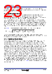
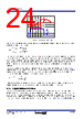
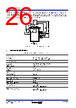
23 / 31 page  R34DS0034EU0101 Rev.1.01 Page 23 Mar 13, 2024 ISL73006SLH Datasheet The temperature coefficient of the ESR can be significant and cause difficulty with this. You need careful evaluation for wide temperature range operations. Consider a combination of Tantalum and MLCC capacitors to achieve high total capacitance with lower ESR. 5.14 Input Capacitor Selection Use a mix of input bypass capacitors to control the voltage overshoot and undershoot across the internal MOSFETs of the synchronous buck regulator. Use small low ESR ceramic capacitors for high-frequency decoupling and bulk capacitors to supply the current needed each time the upper MOSFET turns on. Place the small ceramic capacitors physically close to the IC between the PVIN and PGND pins. The critical parameters for the bulk input capacitance are the voltage and RMS current ratings. For reliable operation, select bulk capacitors with voltage and current ratings above the maximum input voltage and largest RMS current required by the circuit. Their voltage rating should be at least 1.5 times greater than the maximum input voltage, while a voltage rating of 2.5 times is a conservative guideline when considering voltage derating performance to 125°C. Consult the capacitor datasheets for temperature derating tables. For most cases, the RMS current rating requirement for the input capacitor of a buck regulator is approximately 1/2 the DC load current. Use Equation 11 to closely approximate the maximum RMS current through the input capacitors. The minimum recommended input capacitance for the ISL73006SLH is 22µF. Place these high-frequency, low-ESR capacitors close to the VIN and PGND pins. These capacitors provide the instantaneous current into the buck regulator during the high-frequency switching transitions. 5.15 Output Capacitor Selection An output capacitor is required to filter the inductor ripple current and supply the load transient current. The filtering requirements are a function of the switching frequency and the ripple current. The load transient requirements are a function of the slew rate (di/dt) and the magnitude of the transient load current. These requirements are generally achieved with a combination of bulk and decoupling capacitors with a careful layout. High-frequency, low ESR ceramic capacitors initially supply the transient load current and reduce the current load slew rate seen by the bulk capacitors. The Effective Series Resistance (ESR) and voltage rating requirements generally determine the bulk filter capacitor values rather than actual capacitance requirements. Place high-frequency decoupling capacitors as close to the power pins of the load as physically possible. Be careful not to add inductance in the circuit board wiring that could cancel the usefulness of these low inductance components. The shape of the output voltage waveform during a load transient that represents the worst-case loading conditions ultimately determines the number of output capacitors and their type. When this load transient is applied to the regulator, most of the current required by the load is initially contributed by the output capacitors. This is due to the finite amount of time required for the inductor current to slew up or down to the level of the output current required by the load. This results in a momentary undershoot or overshoot in the output voltage. At the initial edge of the transient undershoot or overshoot, the Equivalent Series Inductance (ESL) of each capacitor induces a spike that adds on top of the voltage drop due to the ESR. After the initial spike, the output voltage dips down (load step on) or peaks up (load step off) as the output capacitor sources or sinks the transient load current until the output inductor current reaches the load current. Figure 41 shows a typical response of the output voltage to a transient load current. (EQ. 11) ICINrms VOUT VIN ----------------xIOUT MAX 2 x1 VOUT VIN ---------------- – 1 12 ------x VIN VOUT – LxfOSC --------------------------------x VOUT VIN ---------------- 2 + = |
|
Link URL |
| Does ALLDATASHEET help your business so far? [ DONATE ] |
About Alldatasheet | Advertisement | Contact us | Privacy Policy | Link to Datasheet | Link Exchange | Manufacturer List All Rights Reserved©Alldatasheet.com |
| Russian : Alldatasheetru.com | Korean : Alldatasheet.co.kr | Spanish : Alldatasheet.es | French : Alldatasheet.fr | Italian : Alldatasheetit.com Portuguese : Alldatasheetpt.com | Polish : Alldatasheet.pl | Vietnamese : Alldatasheet.vn Indian : Alldatasheet.in | Mexican : Alldatasheet.com.mx | British : Alldatasheet.co.uk | New Zealand : Alldatasheet.co.nz |
|
Family Site : ic2ic.com |
icmetro.com |
 English ▼
 English
 Chinese
 German
 Japanese
 Russian
 Korean
 Spanish
 French
 Italian
 Portuguese
 Polish
 Vietnamese
 Indian
 Mexican
 British
 New Zealand